Signal Integrity Test Board
Test board implementing various routing topologies. The board can be used for calibrating and comparing measurements of signal propagation properties with Vector Network Analyzers (VNAs). It can also be used for SI, EMI or EMC simulations with field solvers.
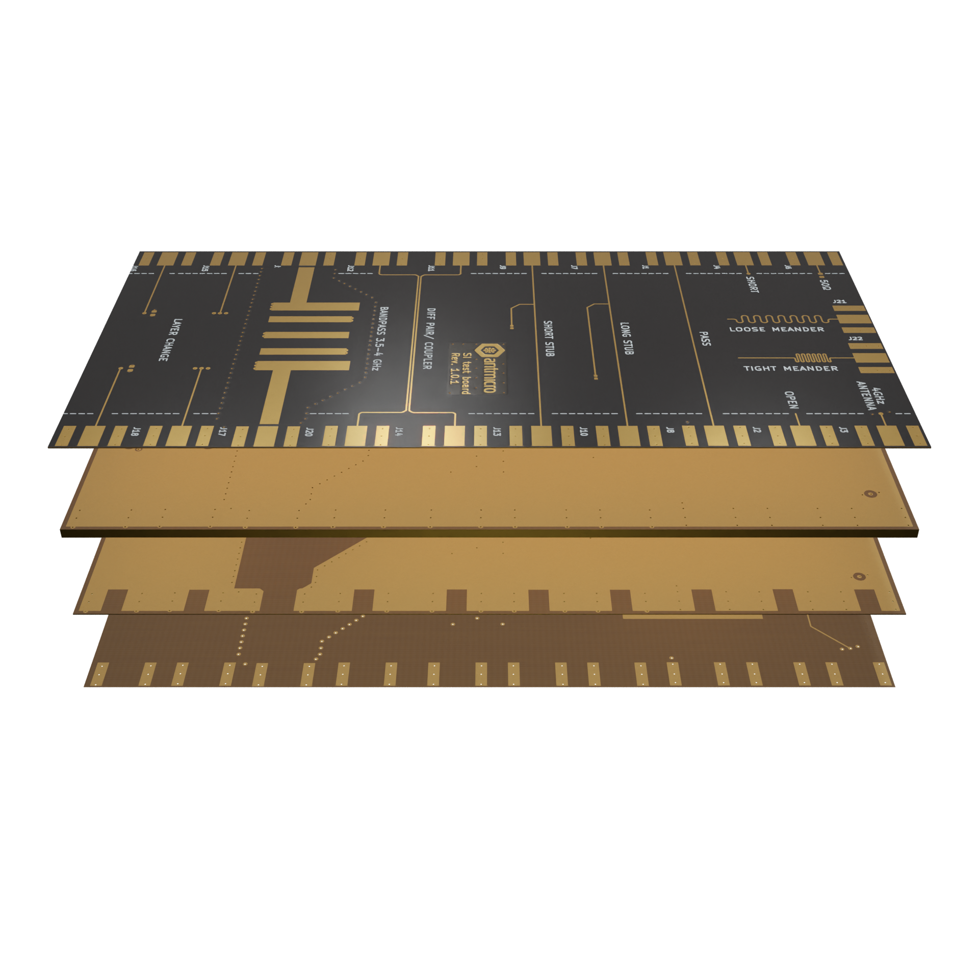
4-layer PCB designed in defined impedance
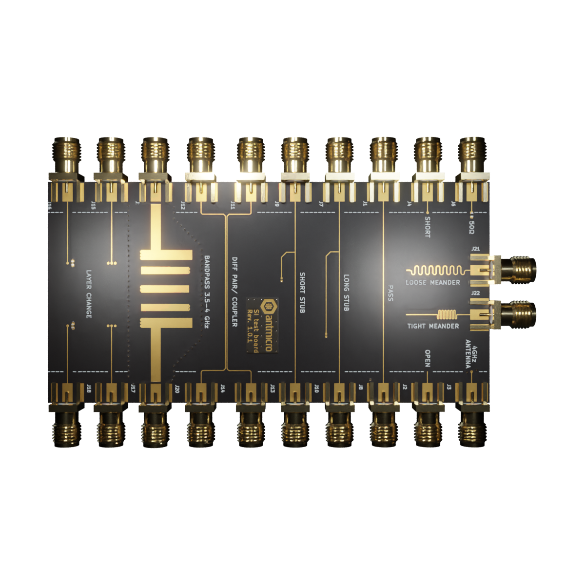
Includes SMA ports connected to copper primitives which implement the following features:
VNA calibration port terminated with 50Ohm
VNA calibration port open (i.e. not terminated)
VNA calibration port shorted (grounded)
Single stripline
Differential pair stripline
Stripline with long stub
Stripline with short stub
Digital bandpass filter
Reference stripline layout with layer-change
Simple planar antenna
Not-terminated striplines with tight and loose meander of the same lengths
Image | Manufacturer | Manufacturer part number | Description | Data available |
|---|---|---|---|---|

Name | Type | Material | Thickness[mm] | Constant |
|---|---|---|---|---|
F.Mask | Top Solder Mask | 0.01 | ||
F.Cu | copper | 0.035 | ||
dielectric 1 | core | FR4 | 0.12 | 4.18 |
In1.Cu | copper | 0.035 | ||
dielectric 2 | prepreg | FR4 | 1.2 | 4.18 |
In2.Cu | copper | 0.035 | ||
dielectric 3 | core | FR4 | 0.12 | 4.18 |
B.Cu | copper | 0.035 | ||
B.Mask | Bottom Solder Mask | 0.01 |


